source:News release time:2023-04-12 Hits: Popular:PCB Assembly company

PCB design refers to the line layout through design drawings to produce circuit boards as low as possible. In the past, this usually requires expensive special tools to complete, but now, with the increasingly popularization of free high -performance software tools and design models, it has greatly accelerated the design speed of circuit board designers.
Although engineering designers know that a perfect design solution is the best way to avoid problems, but this is still a method that is a way to waste time and waste money, and at the same time cure the standard. For example, if problems are found during the electromagnetic compatibility (EMC) testing phase, it will cause a lot of cost investment, and even the initial design plan is needed to adjust and rebuild it, which will take several months.
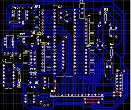
Layout is a problem that designers must face first. This problem depends on some of the content in the drawing, and some devices need to be set together based on logical considerations. However, it should be noted that components that are more sensitive to temperature, such as sensors, should be set separately from components generated by generating calories, including power converters. For design with a variety of power settings, 12 volts and 15 volt power converters can be set in different locations of the circuit board, because the heat and electronic noise they generate will affect the reliability and performance of other components and circuit boards. Essence
The above components will also affect the electromagnetic performance of the circuit design, which is not only very important for the performance and energy consumption of the circuit board, but also has a great impact on the economy of the circuit board. Therefore, all circuit board equipment sold in Europe They must obtain the CE logo to prove that they will not interfere with other systems. However, this is usually only in terms of power supply, and many devices will emit noise, such as DC-DC converters and high-speed data converters. Due to the defects of the circuit board design, these noise can be captured by the channel and radiated as a small antenna, which generates hybrid noise and frequency abnormal areas.
Yuanfang electromagnetic interference (EMI) problem can be solved by adding filters or using metal shells to shield signals at noise point. However, the equipment that can release electromagnetic interference (EMI) on the circuit board fully attaches great importance to it, so that the circuit board can use cheaper shells to effectively reduce the cost of the entire system.
During the design of the circuit board, electromagnetic interference (EMI) is indeed a factor that has to be paid attention to. Electromagnetic spoilers can generate coupling with the channel, which disrupts the signal into noise and affects the overall performance of the circuit board. If the coupling noise is too high, the signal may be completely covered, so a more expensive signal amplifier must be installed to return to normal. However, if you can fully consider the layout of the signal lines at the beginning of the design of the circuit board, the above problems can be avoided. Because the design of the circuit board will be different according to different equipment, different use locations, different heat dissipation requirements, and different electromagnetic interference (EMI), and the design template will be used in handy.
Capacitors are also an important issue in the design of circuit board design that cannot be ignored, because capacitors will affect the speed of the signal and increase the consumption of power. The channel will generate coupling or crossing the two circuit layers vertically, and inadvertently form a capacitor. By reducing the length of the parallel line and adding twisting on one of the lines to cut off the coupling, the above problems can be relatively easy to solve. However, this also requires engineering designer to fully consider the production design principles to ensure that the design plan is easy to manufacture, while avoiding any noise radiation caused by excessive lines of the line. The distance between the lines may also be too close, which will generate a short circuit between the lines, especially the bending of the line. Over time, the metal "beard" will appear. Design rules detection can usually indicate areas where the risk of circuits is higher than normal.
This problem looks particularly prominent in the design of the ground floor. A metal circuit layer may be coupled with all the circuits above and below. Although the metal layer can indeed effectively block noise, the metal layer also generates a accompanying capacitor, affecting the operating speed of the line, and increasing the consumption of power.
As far as the design of multi -layer circuit boards is concerned, the pore design between different circuit board layers is probably the most controversial problem, because Tongkou design will bring many problems to the production and manufacturing of the circuit board. The pores between the circuit board layer will affect the performance of the signal and reduce the reliability of the circuit board design, so they should pay full attention.
Read recommendations:
HASL FR4 Single Sided Copper PCB Board White Solder Mask 35um Thickness
Welcome information, we will answer for you quickly

 No. 1 Jingtian Road, Xinsheng community, Longgang District, Shenzhen, Guangdong, China
 +86 13715096176
 Whatsapp/WeChat : +86 13715096176
 Kevin.kuang@xzgcircuits.com


 Return