source:Other information release time:2023-05-12 Hits: Popular:PCB Assembly company

The design of the printed circuit board is based on the circuit schematic diagram to realize the function required by the circuit designer. The design of the printing circuit board mainly refers to the design of the layout. It is necessary to consider the layout of the external connection, the optimization layout of the internal electronic component, the optimization layout of the metal connection and the pores, the electromagnetic protection, thermal dissipation, and other factors. Excellent layout design can save production costs and achieve good circuit performance and heat dissipation performance. The simple layout design can be implemented by hand. The complex layout design needs to be achieved with a computer -aided design (CAD).
line
Solar Energy System
1. Minimum line width: 4mil (0.1mm). In other words, if the width of the line is less than 6mil, it will not be able to produce. If the design conditions permit, the larger the design, the larger the line width, the larger the factory, the higher the production rate, the general design is about 10mil. consider
2. Minimum line distance: 4mil (0.1mm). The smallest line distance is that the distance from the line to the line, the distance from the line to the pads is not less than 6mil from the perspective of production. The bigger the better. Generally, the conventional conventional is 10mil. Of course, when the design is conditions, the better this point is very important.
3. The distance from the line to the appearance line is 0.508mm (20mil)
via
1. The minimum pore diameter: 0.3mm (12mil)
2. The minimum pores (VIA) pores are not less than 0.3mm (12mil), and the unilateral side of the pads cannot be less than 6mil (0.153mm), and it is best to be greater than 8mil (0.2mm).
3. Pole (VIA) to the pilot distance (edge to the edge of the hole) cannot be less than 6mil, preferably greater than 8mil.
4. Point distance from pads to the appearance line 0.508mm (20mil)
Read recommendations:
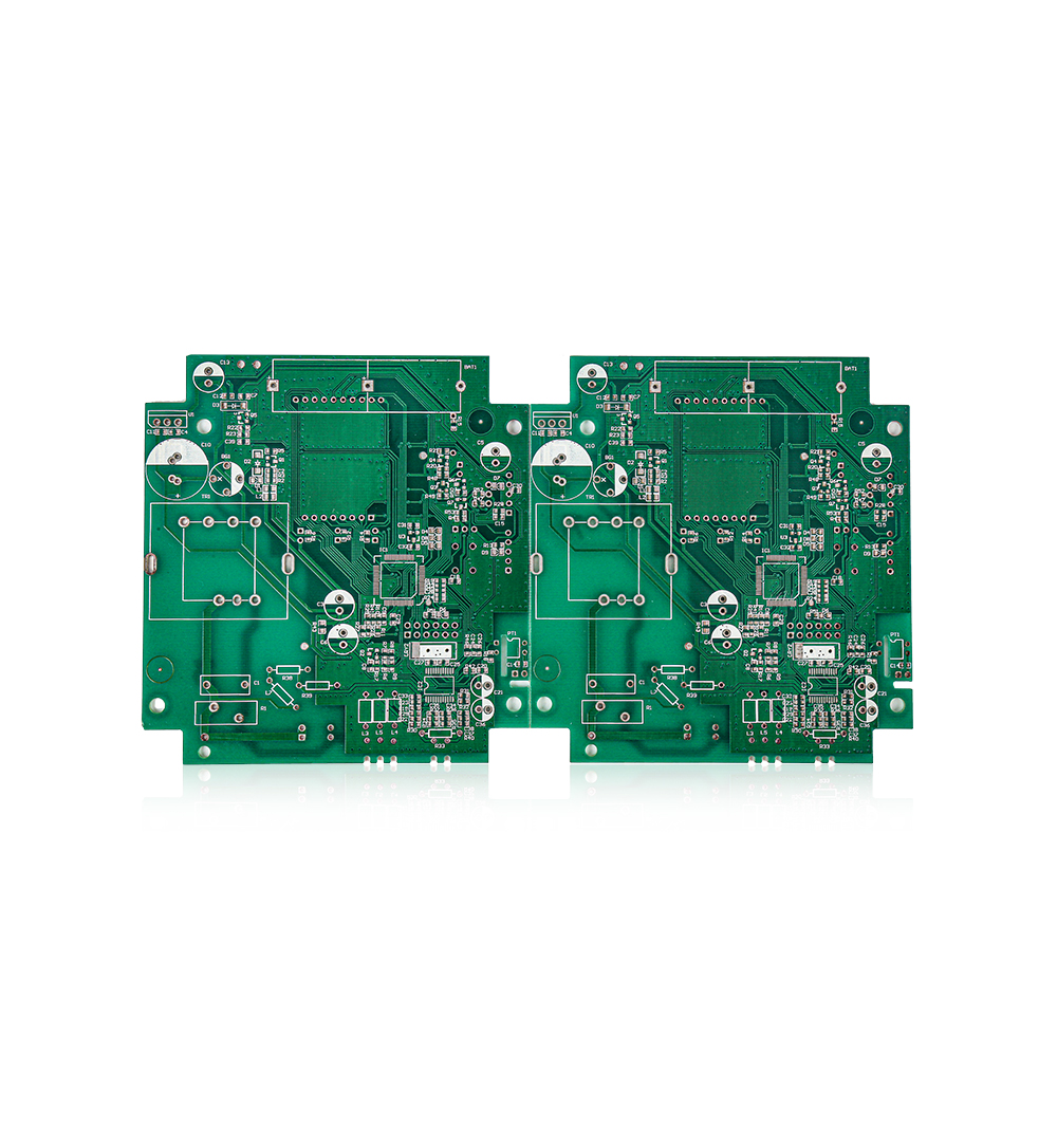
Small BGA Multilayer Printed Circuit Board 6 Layer 3mil Immersion Gold
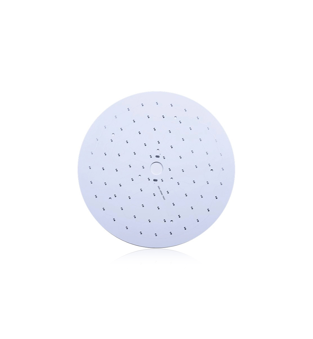
Metal Core 0.8mm Led Street Light Pcb Aluminium Pcb Board For Led
Welcome information, we will answer for you quickly

 No. 1 Jingtian Road, Xinsheng community, Longgang District, Shenzhen, Guangdong, China
 +86 13715096176
 Whatsapp/WeChat : +86 13715096176
 Kevin.kuang@xzgcircuits.com


 Return