source:Other information release time:2023-03-09 Hits: Popular:PCB Assembly company

1) 3mm around the bend/public, curved, and female pressure connection device must not have components higher than 3mm, and there must be no welding device around 1.5mm around; There must be no meta device.
2) 1mm around the direct/public, straight/mother pressure connection device must not have any components; when the back of the straight/public, direct/mother pressure connection device is required, the sheath must not be installed. Device, no meta component is not arranged within a range of 2.5mm from the range of the cover of the cover.
3) European -style connectors with a charged plug -in seat for ground connectors used.
4) 2mmfb power single PIN pins, corresponding to 8mm ban on the front end of the single -board socket.
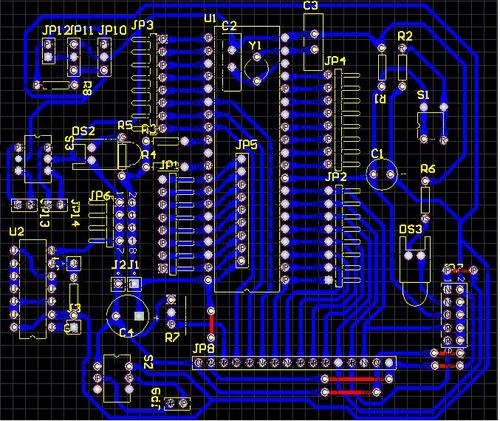
The layout requirements of thermal device
1) During the device layout, the thermal device (such as electrolytic capacitors, crystal, etc.) should be kept away from high heat devices as possible.
2) Thermal device should be close to the measured components and stay away from high -temperature areas, so as not to be affected by other thermal components, causing misunderstandings.
3) Place the heating and heat -resistant device itself at the position or top of the air outlet, but if you cannot bear the higher temperature, you must also put it near the air inlet. Pay attention to as much as possible with other thermal devices and thermal devices in the air to rise in air. Staged in the direction.
Read recommendations:
Multilayer Printed Circuit Board 1OZ 4 Layer Multilayer Pcb FR4 TG170 Blue Solder Mask
Immersion Gold 4 Layer Flex Pcb Rigid Printed Circuit Board 2.0mm 3mil
Welcome information, we will answer for you quickly

 No. 1 Jingtian Road, Xinsheng community, Longgang District, Shenzhen, Guangdong, China
 +86 13715096176
 Whatsapp/WeChat : +86 13715096176
 Kevin.kuang@xzgcircuits.com


 Return