source:Other information release time:2022-11-16 Hits: Popular:PCB Assembly company

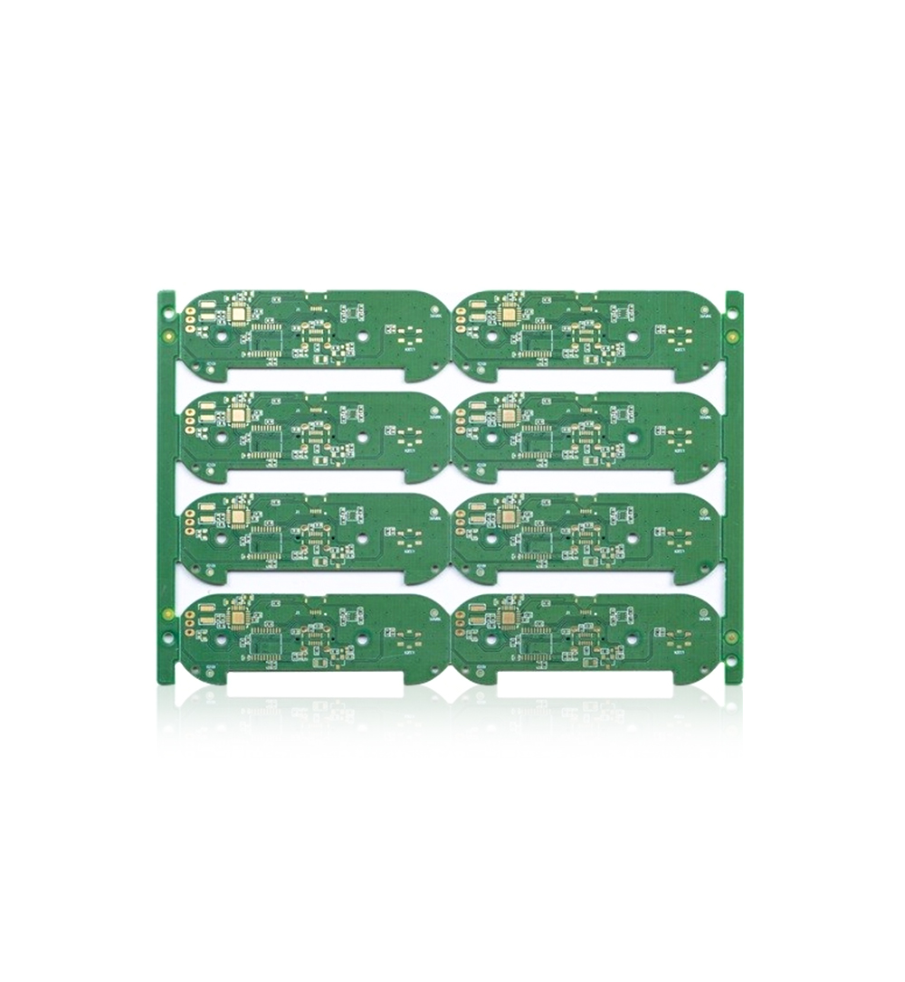
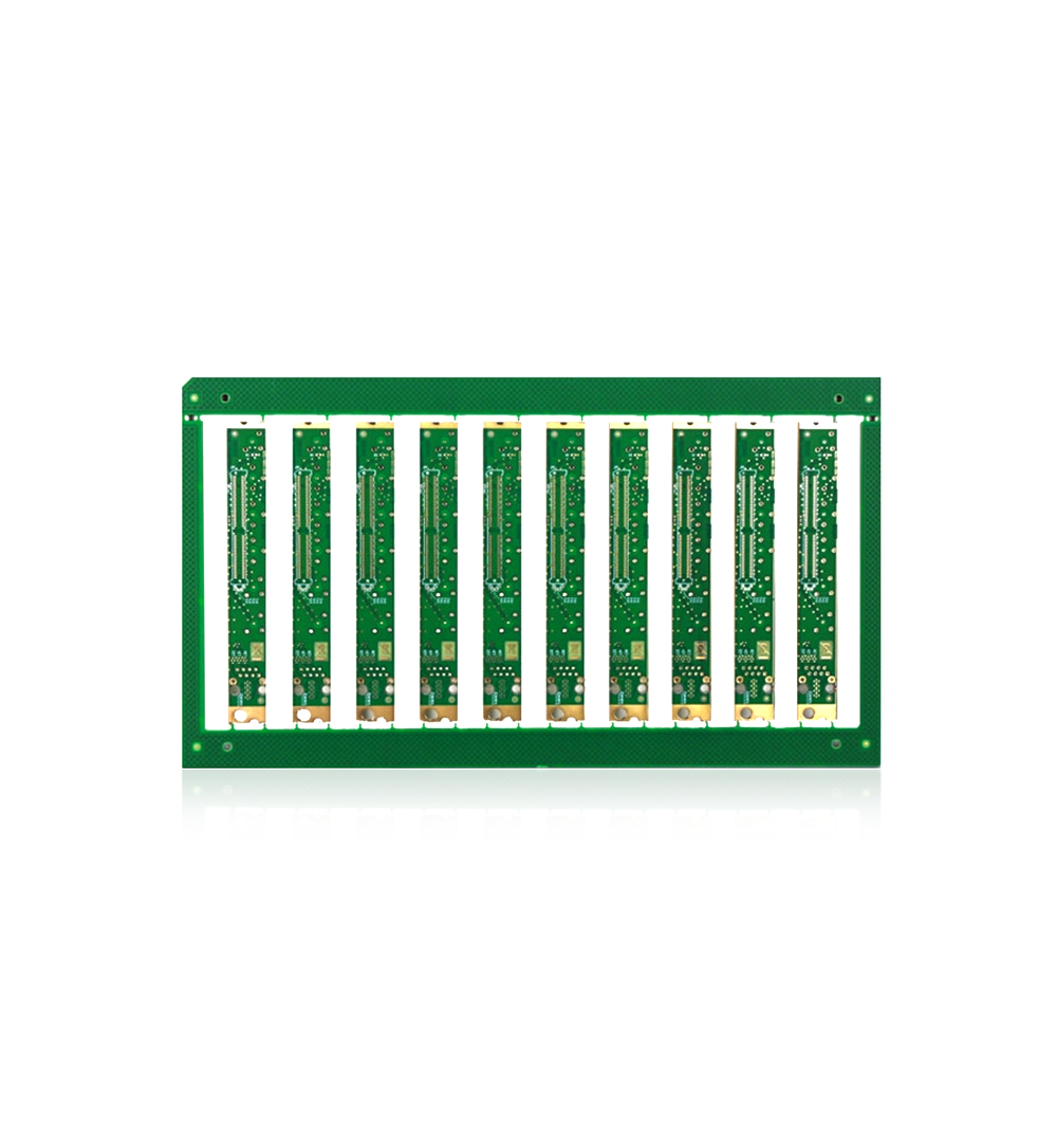
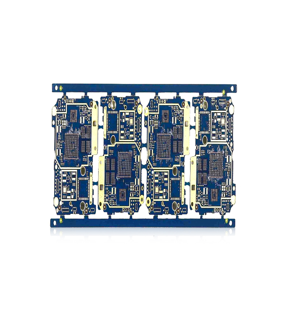
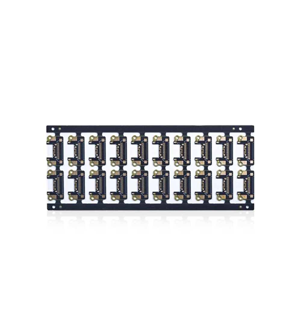
Traditional circuit boards are often divided into single-sided PCB boards, double-sided PCB boards, and PCB multilayer boards, while PCB multilayer boards are divided into single press and multiple press structures. Of course, this kind of design involves some electrical properties and link density problems. However, because of the advanced technology of electronic products, these geometric structures cannot meet the installation density and electrical requirements of components. In order to improve the link density of components, from the geometric point of view, only by compressing the space of lines and connection points can we increase the link density by adding more contacts in the small space. Of course, multiple components can also be stacked in the same position to improve the construction density. Therefore, high-density circuit board is not only a kind of circuit board technology, but also an issue of electronic construction and assembly.
In order to improve the connection density of components, from a geometric point of view, only by compressing the space between lines and connection points, so that more contacts can be accommodated in a smaller space, can the connection density be improved. Of course, there is another different idea, that is, multiple different components can be stacked in the same location to improve the density of the fabric. Therefore, from a certain point of view, high-density circuit boards are not only a technical problem of circuit boards, but also a problem of electronic construction and assembly. I am afraid that it is worth the industry to make some efforts to understand this.
The so-called electronic structure generally refers to the connection between semiconductor chips and carrier plates. The China Road Board Association has published a special book on "Electronic Structure Loader Technology", which can be consulted by those interested. As for the electronic assembly part, it is the work that the components after the electronic assembly are installed on another functional circuit board again. This connection is generally called OLB (outer lead bond), which refers to the connection part of the pin outside the component. The connection of this part is directly related to the surface contact density of electronic components. When the function and integration of electronic products are getting higher and higher, while the demand for mobility, thinness and multifunction is constantly rising, of course, there will be the pressure of high-density.
If high-density circuit board design concept is adopted, electronic products can obtain the following benefits:
1. The high-density circuit board structure adopts thinner dielectric thickness, and the potential inductance is relatively low.
2. The micropores have low aspect ratio, and the signal transmission reliability is higher than that of ordinary through-holes.
3. Micro holes can improve the flexibility of circuit configuration and simplify the circuit design.
4. The same product design can reduce the number of carrier plates, improve the density and reduce the cost.
5. The use of microporous interconnection can shorten the contact distance, reduce signal reflection and crosstalk between lines, and the module can have better electrical performance and signal correctness.
6. Increase the wiring density and increase the line capacity per unit area with microporous thin wires, which can meet the assembly requirements of high-density contact components and facilitate the use of advanced construction.
7. The high-density circuit board microporous technology can shorten the grounding and signal layer distance of the carrier board design, thus improving the RF/electromagnetic wave/electrostatic discharge (RFI/EMI/ESD) interference. The number of grounding wires can be increased to prevent the damage of instantaneous discharge caused by electrostatic accumulation of components.
Read recommendations:
Welcome information, we will answer for you quickly

 No. 1 Jingtian Road, Xinsheng community, Longgang District, Shenzhen, Guangdong, China
 +86 13715096176
 Whatsapp/WeChat : +86 13715096176
 Kevin.kuang@xzgcircuits.com


 Return