source:News release time:2023-02-10 Hits: Popular:PCB Assembly company

The first -order is relatively simple, and the processes and processes are easy to control.
The second order began to cause trouble, one is the problem of the position, the other is the problem of punching and copper plating. There are many second -order design. One is the wrong position of each order. When connecting the secondary neighborhood, it is connected to the middle layer through the wire. The method is equivalent to two first -order HDI line boards. The second is that the two -order holes are overlapped. The second order is achieved by the superposition method, and the processing is similar to the two first -order, but there are many key points of the process, which should be specially controlled, which is mentioned above. The third type is to punch perforation directly from the outer layer to the third layer (or N-2 layer). There are many different techniques from the front, and the difficulty of punching is even more difficult.
It means that the first and the last layer requires drilling holes (usually laser drilling). These holes are mainly drilling the BGA area. The space elsewhere should be sufficient.
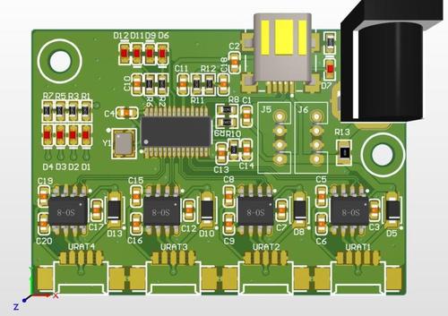
If it is a four-layer line board, it is 1-2 and 3-4 layers
If it is a six-layer circuit board, it is 1-2 and 5-6 layers
As for the buried hole board, it can't be seen. Essence It depends on how specific data engineers are designed.
Read recommendations:
Blue Solder Mask Double Sided PCB Board High TG TG170 S1000-2
Welcome information, we will answer for you quickly

 No. 1 Jingtian Road, Xinsheng community, Longgang District, Shenzhen, Guangdong, China
 +86 13715096176
 Whatsapp/WeChat : +86 13715096176
 Kevin.kuang@xzgcircuits.com


 Return